Anterwell Technology Ltd.
Anterwell Technology Ltd.
Large Original stock of IC Electronics Components, Transistors, Diodes etc.
High Quality, Reasonable Price, Fast Delivery.
Anterwell Technology Ltd.
Large Original stock of IC Electronics Components, Transistors, Diodes etc.
High Quality, Reasonable Price, Fast Delivery.

Product Details:
Payment & Shipping Terms:
|
| Power Supply Voltage: | 40 Vdc | Comparator Input Voltage Range: | −0.3 To +40 Vdc |
|---|---|---|---|
| Switch Collector Voltage: | 40 Vdc | Switch Current: | 1.5 A |
| Operating Junction Temperature: | +150 °C | Storage Temperature Range: | −65 To +150 °C |
| High Light: | electronics ic chip,integrated circuit ic |
||
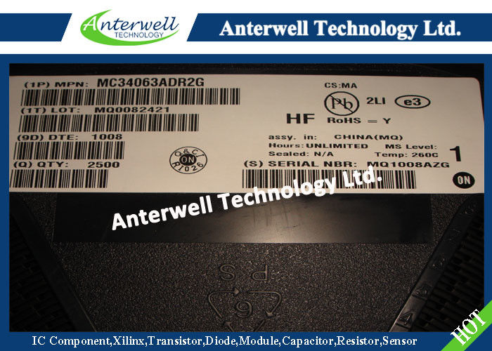
MC34063A, MC33063A, NCV33063A
1.5 A, Step−Up/Down/ Inverting Switching Regulators
The MC34063A Series is a monolithic control circuit containing the primary functions required for DC−to−DC converters. These devices consist of an internal temperature compensated reference, comparator, controlled duty cycle oscillator with an active current limit circuit, driver and high current output switch. This series was specifically designed to be incorporated in Step−Down and Step−Up and Voltage−Inverting applications with a minimum number of external components. Refer to Application Notes AN920A/D and AN954/D for additional design information.
Features
• Operation from 3.0 V to 40 V Input
• Low Standby Current
• Current Limiting
• Output Switch Current to 1.5 A
• Output Voltage Adjustable
• Frequency Operation to 100 kHz
• Precision 2% Reference
• Pb−Free Packages are Available
MAXIMUM RATINGS
|
Rating |
Symbol |
Value |
Unit |
|
Power Supply Voltage |
VCC |
40 |
Vdc |
|
Comparator Input Voltage Range |
VIR |
−0.3 to +40 |
Vdc |
|
Switch Collector Voltage |
VC(switch) |
40 |
Vdc |
|
Switch Emitter Voltage (VPin 1 = 40 V) |
VE(switch) |
40 |
Vdc |
|
Switch Collector to Emitter Voltage |
VCE(switch) |
40 |
Vdc |
|
Driver Collector Voltage |
VC(driver) |
40 |
Vdc |
|
Driver Collector Current (Note 1) |
IC(driver) |
100 |
mA |
|
Switch Current |
ISW |
1.5 |
A |
|
Power Dissipation and Thermal Characteristics |
|
|
|
|
Plastic Package, P, P1 Suffix |
|
|
|
|
TA = 25°C |
PD |
1.25 |
W |
|
Thermal Resistance |
RθJA |
100 |
°C/W |
|
SOIC Package, D Suffix |
|
|
|
|
TA = 25°C |
PD |
625 |
mW |
|
Thermal Resistance |
RθJA |
160 |
°C/W |
|
Operating Junction Temperature |
TJ |
+150 |
°C |
|
Operating Ambient Temperature Range |
TA |
|
°C |
|
MC34063A |
|
0 to +70 |
|
|
MC33063AV, NCV33063A |
|
−40 to +125 |
|
|
MC33063A |
|
−40 to +85 |
|
|
Storage Temperature Range |
Tstg |
−65 to +150 |
°C |
Stresses exceeding Maximum Ratings may damage the device. Maximum Ratings are stress ratings only. Functional operation above the Recommended Operating Conditions is not implied. Extended exposure to stresses above the Recommended Operating Conditions may affect device reliability.
1. Maximum package power dissipation limits must be observed.
2. This device series contains ESD protection and exceeds the following tests: Human Body Model 4000 V per MIL−STD−883, Method 3015. Machine Model Method 400 V.
3. NCV prefix is for automotive and other applications requiring site and change control.
Representative Schematic Diagram
![]()
MARKING DIAGRAMS PIN CONNECTIONS
![]()
![]()
PACKAGE DIMENSIONS
SOIC−8 NB
D SUFFIX
CASE 751−07
ISSUE AG
![]()
PDIP−8
P, P1 SUFFIX
CASE 626−05
ISSUE L
![]()
High Power Rectifier Diode 1N4756A , Silicon Planar Zener Diodes
Bridge Type Rectifier Diode 1N4007 50 to 1000 Volts 1.0 Ampere
1N4742A Silicon Planar Zener Diodes for Stabilized Power Supply
Power Programmable IC Chips XC6SLX100-3FGG484C Spartan-6 Family Overview
128K Bytes Sound IC Chip Programming ATMEGA128-16AU 8 Bit Microcontroller
EMC Programmable IC Chips Compliant Slew Rate Limited EI , Timer IC Chip
SMD Power Mosfet Module L7812CV TO-220 Power Trans Electronic Compoents
2SD1594 3 Pin Transistor NEC NPN Power Transistor Switching High Speed
2N5459 Power Mosfet Transistor N-Channel To-92 Original Stock FSC